Supports Large Sensors up to 16k/5u

Low magnification autofocus system

Low Magnification Semiconductor
Autofocus System AOI

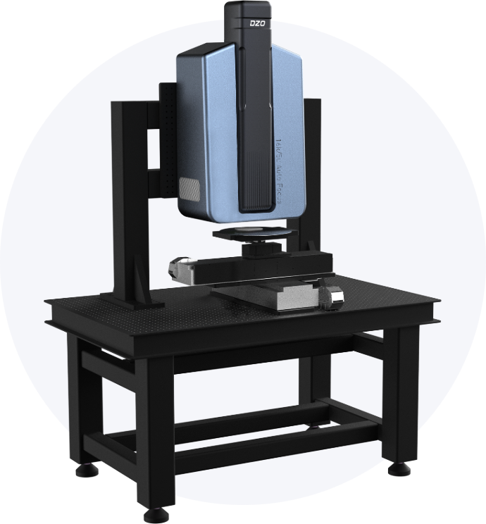
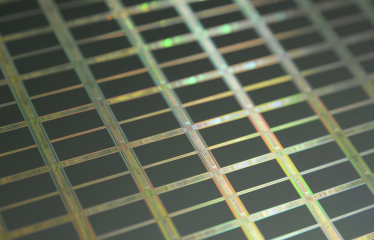
With the booming development of industries such as smart terminals, wireless communication and network infrastructure, smart driving, cloud computing, and smart healthcare, the critical size of advanced integrated circuits has further shrunk to sub-10nm scale, and the identification, localization, and classification of fabrication defects on patterned wafers have become increasingly challenging. And the low magnification semiconductor autofocus system of DZOPTICS is just able to correspond to a series of problems on wafers.

Areas Of Application
Patterned/Unpatterned Wafer Inspection
Panel Inspection
IC Carrier Board Inspection

Product
Parameters

sports event
Focus stroke/time
Focusing accuracy
Motor frequency
Rangefinder Camera Calculation Frequency
Encoder resolution
Motor Positioning Accuracy
Motor Stroke
Z-axis maximum load
Gauge Weight
Instrument size (mm)
norm
±0.5mm/<100ms
1/4x depth of field
40Hz
330Hz
0.1um
士1um
10mm
22kg
30kg
L:495*W795*H:255

Technical Advantages

Supports Large Camera Target Surface 16k/5u
Lens Large Na Design For High Light Throughput
and High Resolution;
Focusing and imaging sections are independent of each other, lens magnification can be changed
Line laser focusing, to avoid abnormal focusing caused by the product's individual position bulge
High-speed rangefinder camera, real-time autofocus, supports line frequency of 250khz or more
Low magnification semiconductor autofocus system AOI (manual)
download