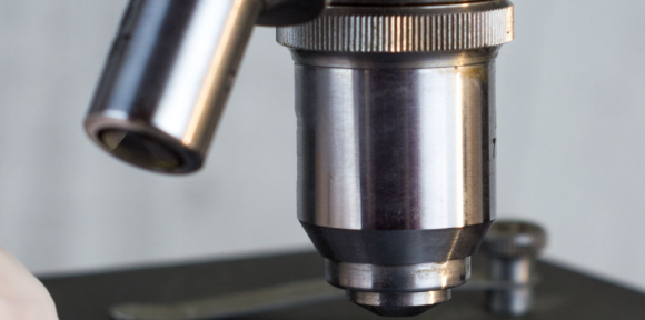
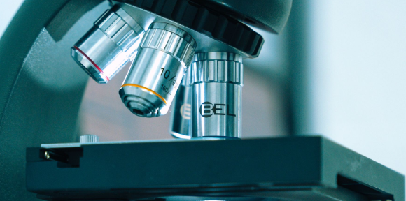
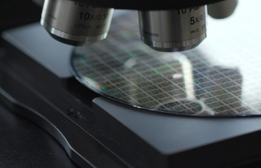
Supports 5x-100x Objective Lenses

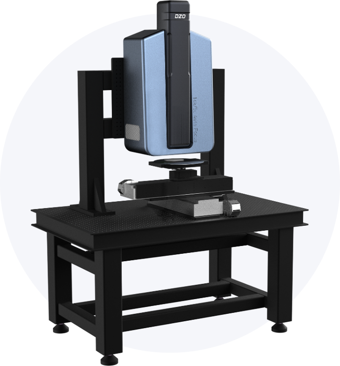
High-Precision & Wide Working Distance Range Laser Autofocus Mode

High-Magnification Semiconductor
Autofocus System AOI

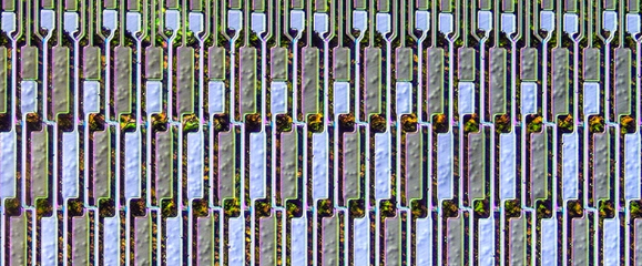
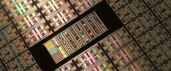
AOI inspection is not just a piece of inspection equipment, a large number of bad results for classification and statistics, you can find the reasons for the occurrence of bad, in process improvement and production yield enhancement is also gradually playing a more important role, our high-frequency semiconductor autofocus system AOI, electronic components, semiconductor defects, and so on neighboring areas have more than one solution.

Application Areas
Wafer Defect Inspection
OLED Defect Inspection
IC Substrates Inspection
MicroLED Defect Inspection

Products
Parameters

norm
Magnification
Depth of Field
Laser Focus Range
Laser Focus Frequency
Focusing Accuracy
Focusing Method
Laser Wavelength
Beam Shape
Laser autofocus cycle time
Objective lens switching time
Objective switching accuracy
Dimension
Working Temperature
Weight
Target size
With Plan APO infinity microscope objective lens
5x 10x 20x 50x 100x
14μm 3.5μm 1.6μm 0.9μm 0.6μm
12mm 4mm 1.5mm 0.5mm 0.15mm
5KHz
max 0.25x objective depth of field
Coaxial laser follow focus
670nm line laser
45° inclined line laser
<0.1s
<0.5s
0.5um
285mm*525mm*210mm
5~50℃
13kg
Image format support φ30mm

Technical Advantages

High-precision, wide working distance range laser autofocus
mode, supports 5x~100x objective lens
The addition of an objective lens switcher allows for the support of up to 5 objective lens switching.
Minimized size and weight due to compact design.
Can be customized according to
customer requirements
High-magnification semiconductor autofocus system AOI (brochure)
download