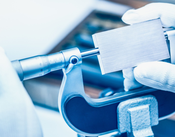
Your Partner For Multidimensional
Industrial Quality Solutions

In many industries where accuracy, quality and efficiency are essential to success, TOHO's
measurement technology ensures that these industries achieve exceptional results.

Industrial Measurement and Quality Inspection

In 3C surface inspection, touch screen manufacturing, AOI optical inspection, PCB printed circuits, silicon wafer sorting, battery wafer process inspection and sorting based on professional optical technology knowledge to provide our customers with products and related services support.

Optical Technology Use Cases

Main application lenses: line scan lenses
Common defects: cracks, missing corners, color abnormalities, spots, segment grids.

Line Scan Lens - In the photovoltaic industry, DZO can provide manufacturers with multiple production links, mature and efficient vision solutions. Silicon wafer appearance defects detection, cell appearance inspection, cell EL inspection, insulation sheet positioning and positional degree detection, etc. DZO launched more than 40 kinds of high-quality lenses that can be matched with (full-frame) cameras, 4K, 8K, 16K line-scan cameras. The products have ultra-low distortion, resolution up to 200LP/mm, and magnification covering 0.04x to 6.2x. Compared with European, American and Japanese lenses, DZO line scan products have a very high cost performance.

Optical Technology Use Cases

Main application lenses: Macro lenses Common
defects: flaws stains, cosmetic defects, missing corners.

When scanning the code of each production section process processing, through the industrial camera will product ID QR code information recognition and extraction, to track inventory capacity, production process information and product quality can help enterprises to grasp the digital information related to the production process, quickly locate the problem and prevent risks, and to facilitate the enterprise to improve the reliability and safety of the product. dzo optimized for the current market demand of customers. DZO has designed a series of macro lenses. Optical distortion as low as 0.05% plane detection comparable to telecentric high-precision detection, variable aperture.

Optical Technology Use Cases

Main application lenses: telecentric lenses Common
defects: soldering abnormalities, component reversal/offset, lead damage.

Telecentric lens - in the field of PCB welding inspection requirements are usually very fine pitch and high density, so the requirements of the optical lens is not only in the resolution of the sharpness of the demand is very high, the scene picture stitching needs to also have a high demand. Ordinary industrial lenses are difficult to meet the AOI inspection requirements, so it is necessary to choose the telecentric lens to go with the entire system of inspection applications.DZO optimized for the needs of high-end users to design a unique telecentric lens, the user can get a more high-definition and ultra-low distortion visual processing image when using DZO telecentric lens products support 5-12 million resolution products covering 2/3 inch to 1.75 inch all the cameras.

Optical Technology Use Cases

Main application lenses: line scanning lenses Common
defects: point defects, line defects, MURA defects.

With the rapid development of electronic technology, image sensing technology and deep learning technology, the use of machine vision-based surface defects automatic optical (vision) inspection technology to replace the manual visual detection of surface defects, has gradually become an important means of surface defect detection, because this method has the advantages of automation, non-contact, fast speed, high precision, high stability. DZO launched more than 40 kinds of high-quality lenses that can be matched with (full-frame) cameras, 4K, 8K, 16K line scan cameras. It can meet the different needs of customers.

Optical Technology Use Cases

Main application lens: line scanning lens Common
defects: leakage of foil, bright and dark marks, bad coating, misalignment.

As the raw material for lithium battery production, the battery pole piece is prone to many different types of defects such as cracks, spots, scratches and other defects during the production process due to coating, rolling, welding, etc., which affects the performance and quality of the product, and therefore it is necessary to strengthen the detection of surface defects on the lithium battery pole piece. Line scanning lens can effectively obtain the actual edge of the pole piece, to get the ideal pole piece contour of the accurate image information, to eliminate the inaccurate positioning to the stacking and packaging and other aspects of the safety risks.

Optical Technology Use Cases

Main application lenses: line scan lenses Common
defects: contamination, scratches, residual metal, photoresistor residue, impact damage, etc.

PCBs go through several processes, and manufacturing and visual inspection points are critical throughout the process. Line scan lenses can be used in circuit print film inspection, inner layer etch inspection, outer layer etch inspection, final PCB inspection and more. Can help PCB manufacturers detect defective boards with up to 98% accuracy. Reduces labor by more than 50%.

Photovoltaic Application
Cases
Scanning Use
Cases
3D AOI Optical Inspection
Application Case
Screen Application
Cases
Lithium
application cases
PCB Printed Circuit
Application Examples

2D Detection

(VR IR optical detection)

Augmented Reality (AR) Virtual Reality (VR) devices are rapidly growing in a wide range of applications in life,
from R&D labs to different sites in daily life. The applications range from R&D labs to different sites in daily life, including gaming and entertainment, product design and development, equipment maintenance/repair, and distance education and training. The upgrading and application of these products urgently requires the support of optical testing equipment to provide professional testing and evaluation.

Unique Measurement Standards

Lens spatial aberration correction
Luminance uniformity analysis
Defect analysis (dotted lines, mura, etc.)
MTF Analysis

Laser Triangulation

Measurement principle: A laser-generated beam is projected onto the surface of the object to be measured, and the laser spot on the surface of the object is imaged. The processor determines the imaging laser's position on the camera and calculates the distance from the sensor to the object surface. The triangulation sensor's laser effectively produces a small, intense and precisely focused beam, reducing the camera's exposure time and thus effectively eliminating errors due to blurring of the object's motion.

VR Solutions

NASA Space Shooting Program - May 2022 delivered 18 imaging
Highly consistent VR190. field of view up to 190°, 220°, distortion as low as 0.3%, supports M4/3 interface. Applied to aerospace grade precision optics VR180°, 360° panoramic stitching shooting.

Diameter Gauge

Stable measurement of object thickness, height, inner and outer diameters, travel, vibration, deviation, contour, etc. with high accuracy is realized by optical principle. It can be applied to auto body, electric vehicle parts, thin film, semiconductor, medical, electrical and electronic parts, cable/fiber optic and steel.